
Product Overview
The LEx is a high-performance 32-bit Bluetooth® Low Energy (LE) SoC, operating at a 64MHz frequency, high-speed embedded memories (up to 1024KB of Flash memory and up to 64KB of SRAM), and supports the BLE 5.0/5.1 protocol stack.The devices has characteristics such as ultra-low power, high performance, high security, and high reliability. It has industry-leading communication distance, excellent RF performance, and strong anti-interference ability, and supports multiple Bluetooth MESH applications. The LEx suitable for a wide range of IoT applications such as smart homes, smart wearables, medical electronics, industrial control and so on.
General Characteristic
UP To 64MHz
Supports BLE MESH
RX: -99.7@1Mbps
TX: +13dBm(MAX)
ESD HBM≥8KV
Standby Current 1.1uA
Supports 14-channels TK
10V dynamic CS
Rich peripheral interfaces
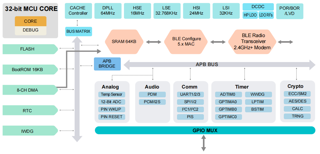
Block Diagram
Key Features
Product Selection Table
| Part ID | BLE | SRAM(KB) | Flash(KB) | GPIO | Timer | UART | SPI | I²C | ADC | TK | Temp | Package |
|---|---|---|---|---|---|---|---|---|---|---|---|---|
| LE5010AI | 5.0 | 64 | 512 | 21 | 5 | 3 | 2 | 2 | 5 | - | -40~85℃ | QFN32 |
| LE5010AJ | 5.0 | 64 | 512 | 21 | 5 | 3 | 2 | 2 | 5 | - | -40~105℃ | QFN32 |
| LE5010BI | 5.0 | 64 | 512 | 34 | 5 | 3 | 2 | 2 | 9 | - | -40~85℃ | QFN48 |
| LE5010BJ | 5.0 | 64 | 512 | 34 | 5 | 3 | 2 | 2 | 9 | - | -40~105℃ | QFN48 |
| LE5010SI | 5.0 | 64 | 512 | 9 | 5 | 3 | 2 | 2 | 2 | - | -40~85℃ | SOP16 |
| LE5110AI | 5.1 | 64 | 512 | 21 | 5 | 3 | 2 | 2 | 5 | - | -40~85℃ | QFN32 |
| LE5110BI | 5.1 | 64 | 512 | 34 | 5 | 3 | 2 | 2 | 9 | - | -40~85℃ | QFN48 |
| LE5020AI (MJIA) | 5.0 | 64 | 512 | 21 | 5 | 3 | 2 | 2 | 5 | - | -40~85℃ | QFN32 |
| LE5020BI (MJIA) | 5.0 | 64 | 512 | 34 | 5 | 3 | 2 | 2 | 9 | - | -40~85℃ | QFN48 |
| LE5030BID | 5.0 | 64 | 512 | 34 | 5 | 3 | 2 | 2 | 9 | - | -40~85℃ | QFN48 |